Google unveils two new TPUs designed for the "agentic era"
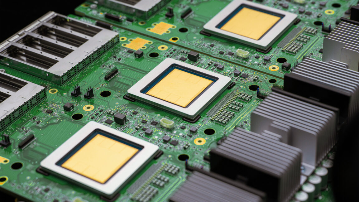
```json { "title": "Google Unveils TPU 8t and 8i for the Agentic AI Era", "metaDescription": "Google launches two new TPUs at Cloud Next 2026: the TPU 8t for training and TPU 8i for inference, built for the demands of agentic AI workloads.", "content": "<h2>Google Splits Its TPU Lineup for the First Time, Targeting the Agentic AI Era</h2><p>At Google Cloud Next 2026 in Las Vegas on April 22, 2026, Google unveiled its eighth-generation Tensor Processing Units — and for the first time in the product line's history, that means two distinct chips rather than one. The <strong>TPU 8t</strong> is purpose-built for large-scale AI model training, while the <strong>TPU 8i</strong> is engineered for high-concurrency AI inference. Together, they represent what Google is calling its architecture for the \"agentic era\" — a period defined by AI systems that take sequences of autonomous actions rather than simply responding to individual prompts.</p><p>The announcement marks a deliberate departure from the seventh-generation Ironwood TPU, which was a single unified platform introduced at Google Cloud Next 2025 and designed primarily for inference. That chip scaled to 9,216 chips per pod and delivered 42.5 exaflops of compute. Its successors, developed in partnership with Google DeepMind over roughly two years of internal development, are built on the premise that training and inference now have fundamentally different — and increasingly irreconcilable — hardware requirements.</p><h2>TPU 8t: Scaling AI Training to One Million Chips</h2><p>The TPU 8t is Google's answer to the raw computational demands of training frontier AI models. A single TPU 8t superpod scales to 9,600 chips — slightly more than Ironwood's 9,216 — and carries two petabytes of shared high-bandwidth memory with double the interchip bandwidth of its predecessor. The chip delivers 121 exaflops of FP4 compute performance per pod, with per-pod compute performance nearly tripling compared to Ironwood. Google claims the TPU 8t delivers up to 2.7 times the performance-per-dollar improvement of Ironwood for large-scale training workloads.</p><p>Reliability during training runs is a central design consideration. The TPU 8t is engineered for over 97% \"goodput\" — the ratio of productive computing time to total uptime. Google notes that a 1% reduction in goodput can translate to days of additional training time at scale, making this metric as consequential as raw compute numbers for production deployments.</p><p>To support massive distributed training, Google built a new network architecture called the <strong>Virgo Network</strong> for the TPU 8t. Built on high-radix switches that reduce network layers, Virgo supports a 4x increase in data center bandwidth and allows up to 134,000 TPU 8t chips to operate as a single fabric within a single data center. Using Virgo Network in combination with Google's JAX and Pathways software, Google can now scale to more than 1 million TPU 8t chips in a single logical training cluster spanning multiple data centers — a figure that represents a new benchmark for distributed AI infrastructure.</p><h2>TPU 8i: Low-Latency Inference for Millions of Concurrent Agents</h2><p>The TPU 8i takes a different architectural path, one shaped by the specific demands of agentic AI inference. A single TPU 8i pod scales to 1,152 chips and delivers 11.6 exaflops of FP8 compute performance, with a total HBM capacity of 331.8TB per pod and 19.2Tbps of bidirectional scale-up bandwidth per chip. Google reports the TPU 8i delivers 80% better performance-per-dollar compared to Ironwood.</p><p>One of the most notable hardware choices in the TPU 8i is its on-chip SRAM allocation. Each chip carries 384 megabytes of on-chip SRAM — triple the amount found in Ironwood — a design decision aimed at reducing processor idle time by keeping frequently accessed data closer to compute. The chip also pairs 288GB of HBM memory alongside that SRAM capacity.</p><p>To address the latency bottlenecks that agentic AI workloads introduce, Google engineered two new systems specifically for the TPU 8i. The first is the <strong>Collectives Acceleration Engine (CAE)</strong>, an on-chip reasoning system that handles the reduction and synchronization steps required during autoregressive decoding and chain-of-thought processing. Google says the CAE reduces on-chip latency by up to 5x. The second is a new network topology called <strong>Boardfly ICI</strong>, which replaces the 3D torus topology used in previous generations and reduces the maximum network diameter by more than 50%, resulting in up to 50% latency improvement.</p><p>Both the TPU 8t and 8i run on Google's custom Axion Arm-based CPUs — with the TPU 8i configuration doubling the physical CPU hosts per server — support liquid cooling technologies, and deliver up to 2x better performance-per-watt compared to Ironwood.</p><h2>Why Google Split Its TPU Line — and What It Signals for AI Infrastructure</h2><p>The decision to bifurcate the TPU lineup is rooted in a recognition that the requirements of training and inference are diverging as AI systems grow more complex. Training demands maximum throughput, linear scalability across thousands of chips, and sustained high utilization over long runs. Inference for agentic AI — where systems may be running millions of concurrent reasoning chains — demands something fundamentally different: low latency, high memory bandwidth at the chip level, and fast synchronization between chips during real-time decoding.</p><p>The move also aligns Google with a broader industry trend. AWS has similarly segmented its custom silicon portfolio into Trainium for training and Inferentia for inference. Google's architectural split puts it in a comparable position to its cloud infrastructure rival, even as both companies compete directly with Nvidia's GPU ecosystem for AI workloads.</p><p>The chips were developed in partnership with Google DeepMind, with Google citing internal discussions about where AI was headed and where future hardware bottlenecks would emerge. According to IT Pro, that internal development process spanned approximately two years before today's announcement.</p><p>Both chips will be generally available later in 2026 and will be accessible as part of Google's <strong>AI Hypercomputer</strong>, a cloud-based supercomputer architecture the company launched in 2023.</p><h2>What Industry Adoption Looks Like Today</h2><p>Google's TPU ecosystem has already attracted significant enterprise and research commitments. Citadel Securities has built quantitative research software that draws on Google's TPUs. All 17 U.S. Energy Department national laboratories use AI co-scientist software built on the chips. And Anthropic has committed to using multiple gigawatts worth of Google TPU capacity going forward.</p><p>These deployments span a range of workload types — from latency-sensitive financial modeling to large-scale scientific research — illustrating the breadth of use cases the eighth-generation architecture is intended to serve.</p><h2>In Their Own Words: Google on the Eighth-Generation TPUs</h2><p>Amin Vahdat, Google's SVP and Chief Technologist for AI and Infrastructure, described the broader significance of the announcement: <em>"Our eighth-generation TPUs are the culmination of more than a decade of development."</em></p><p>Vahdat also articulated the core design philosophy that has guided TPU development since its inception: <em>"The key insight behind the original TPU design continues to hold today: by customizing and co-designing silicon with hardware, networking, and software, including model architecture and application requirements, we can deliver dramatically more power efficiency and absolute performance."</em></p><p>On the specific rationale for splitting training and inference into separate architectures, Vahdat said: <em>"With the rise of AI agents, we determined the community would benefit from chips individually specialized to the needs of training and serving."</em></p><p>The full-stack integration — from chip to network to software — was highlighted as a key competitive advantage: <em>"By owning the full stack, from Axion host to accelerator, we can optimize system-level energy efficiency in ways that simply cannot be achieved when the host and chip are designed independently."</em></p><p>Vahdat also addressed the network topology shift that underpins the TPU 8i's inference performance: <em>"One of the things that we've had to realize is that the way that we were connecting the chips together, the network topology… our default way of connecting them together didn't support latency, it supported throughput, it supported bandwidth."</em></p><p>Thomas Kurian, CEO of Google Cloud, framed the split as a natural evolution rather than a pivot: <em>"For us, it's a natural evolution. We've been working on these chips and systems for multiple years now. And so when AI came along with particularly generative AI became, you know, widespread, we felt that people would want systems that were more optimized for training, and separately, systems that were more optimized for inference."</em></p><h2>What Comes Next</h2><p>Both the TPU 8t and TPU 8i are expected to reach general availability later in 2026. They will be accessible through Google's AI Hypercomputer architecture, which provides cloud-based access to Google's custom silicon and associated software stack. The timeline for broader rollout has not been specified beyond that window.</p><p>The scale benchmarks Google is citing — particularly the ability to orchestrate more than 1 million TPU 8t chips in a single logical training cluster — suggest the company is positioning this generation to support model training at a scope that current public AI systems have not yet reached. Whether those benchmarks translate into measurable gains for the research and enterprise customers who will actually deploy these chips remains to be seen when availability opens later this year.</p><p>For more tech news, visit our <a href=\"/news\">news section</a>.</p><h2>Why This Matters for Health and Productivity</h2><p>The infrastructure powering the next generation of AI agents isn't an abstract concern — it directly shapes the tools that professionals, researchers, and health-focused platforms will use to work smarter. Faster, more efficient inference chips like the TPU 8i mean AI assistants and productivity tools can run more complex reasoning in real time, at lower cost, making agentic AI features more accessible across industries. As these capabilities filter into health and productivity applications, staying informed about the hardware that makes them possible is increasingly relevant to anyone optimizing how they work and live. Join the <a href=\"/#waitlist\">Moccet waitlist</a> to stay ahead of the curve.</p>", "excerpt": "Google unveiled two new eighth-generation TPUs at Cloud Next 2026: the TPU 8t for large-scale AI training and the TPU 8i for high-concurrency inference. It marks the first time Google has split its TPU lineup into architecturally distinct chips, a move designed to meet the divergent demands of the agentic AI era. Both chips are expected to reach general availability later in 2026.", "keywords": ["Google TPU 8t", "Google TPU 8i", "agentic AI chips", "Google Cloud Next 2026", "AI training inference hardware"], "slug": "google-tpu-8t-8i-agentic-era-cloud-next-2026" } ```